Warpverter
A Serious Electronic Project For The Expert DIYer
How It Works
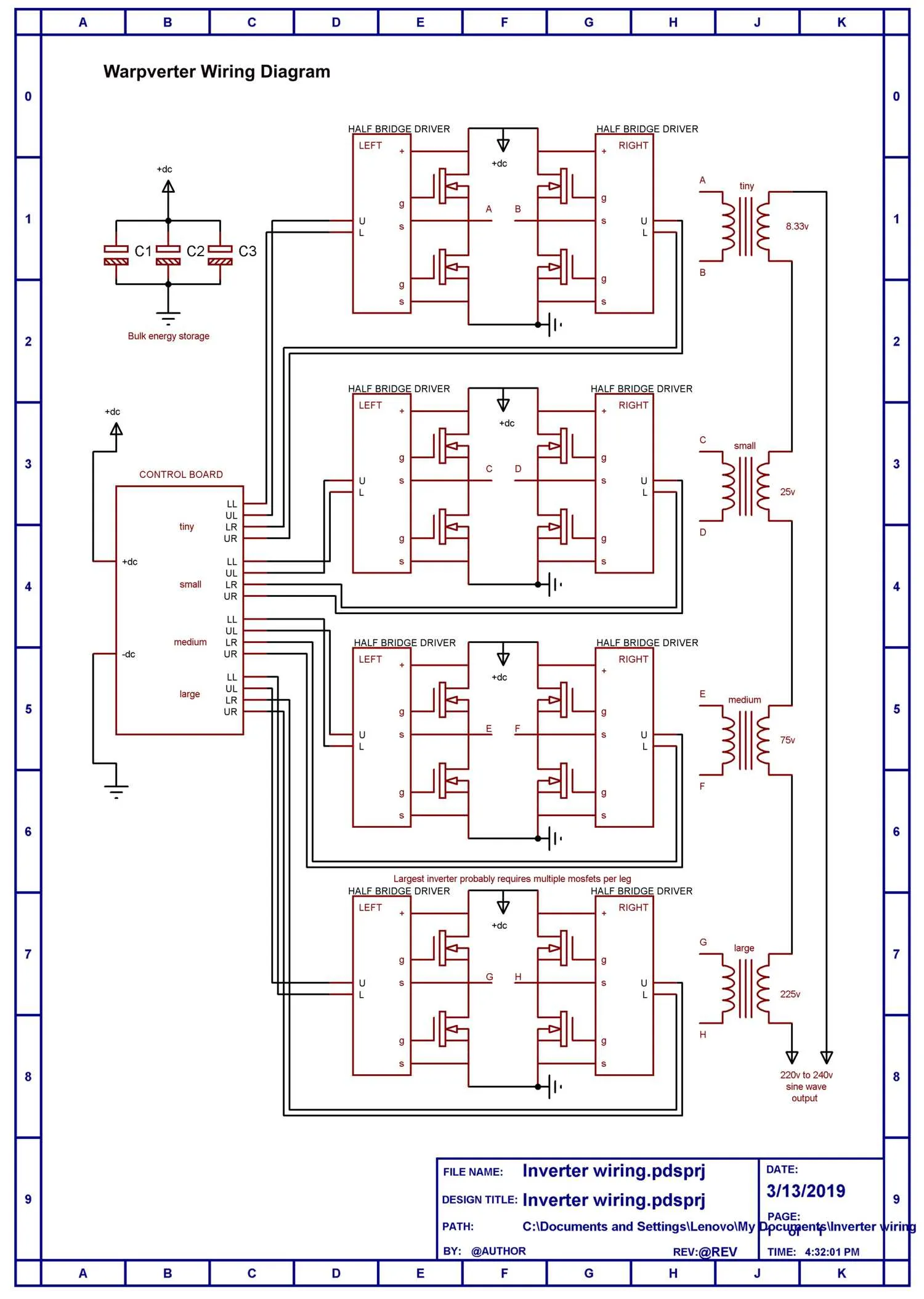
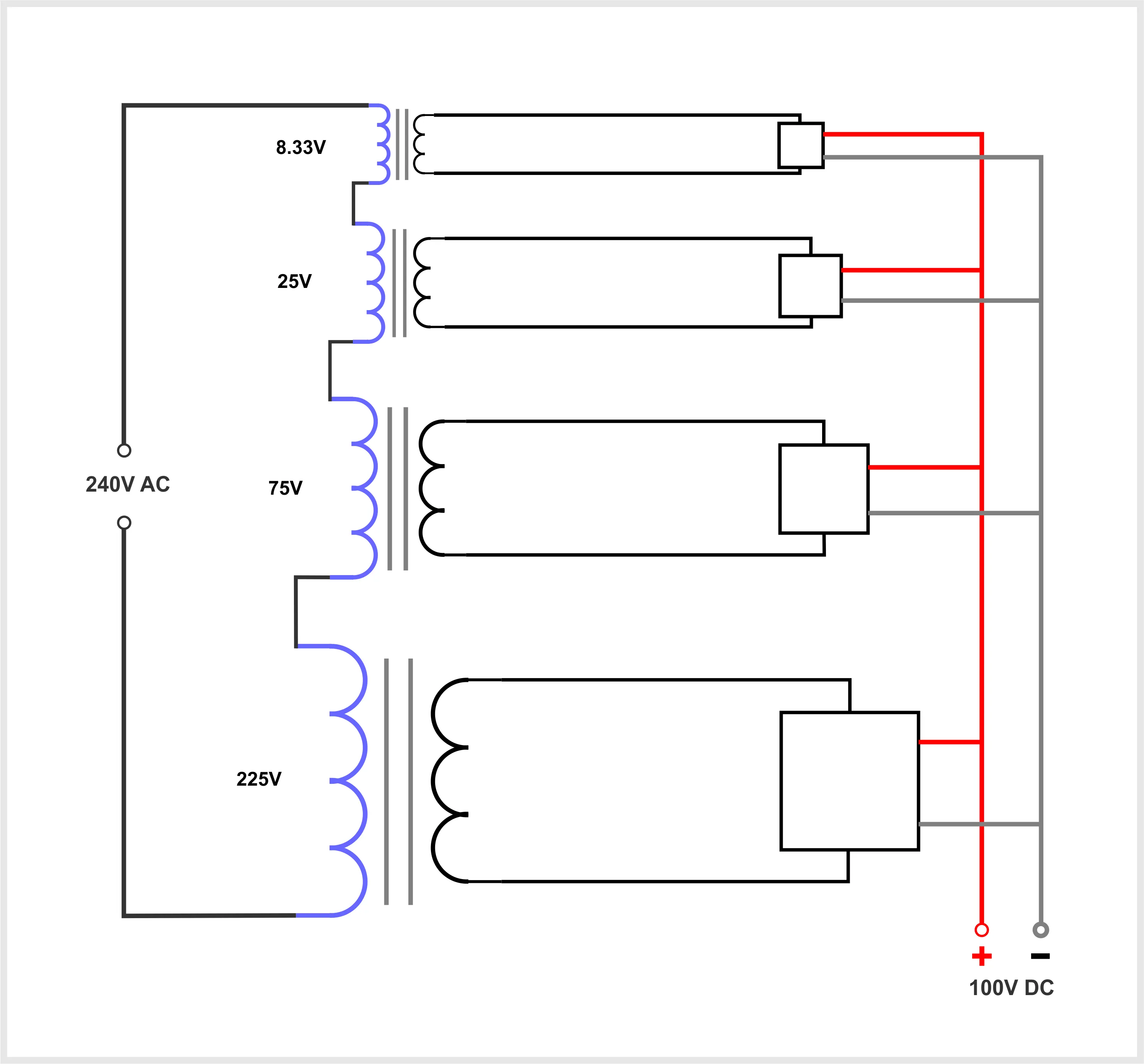
A Warpverter combines the output of four low frequency square wave inverters.
Each of these inverters has an output transformer that has a different secondary voltage.
The four secondaries are connected in series to directly generate an analogue ac sine wave.
It’s rather like a direct digital to analogue conversion at hundreds of volts and thousands of watts.
Each square wave inverter has potentially three output states +ve, zero, and -ve.
There are four inverters (four bits).
Four bits of binary can only produce 2 x 2 x 2 x 2 = 16 output voltage levels.
But …
Four bits of "trinary" can produce 3 x 3 x 3 x 3 = 81 output voltage levels.
That is an 81 step peak to peak sine wave, forty steps up, zero, and forty steps down.
Many thanks to Paweł Sroczyński, www.enklava.co project for this Warpverter Simulator
Warpverter Block Diagram
“ I developed this gradually myself over many years. The original prototypes all used various microcontrollers to generate the required switching waveforms. But I gradually simplified it down to be an all hardware design (no software crashes !) “
Tony Le Grip
There are quite a few hidden features in all of this, that may not be immediately obvious.
Firstly it’s not too difficult to see how switching the primaries generate the required three level rectangular voltage waveforms in the secondaries, and how the series connected secondaries all add these together directly, to generate a very low distortion sine wave output voltage.
The measured THD is 0.85% and the strongest harmonic is the third which is down -40db.
What may be less obvious, is that the sine wave current in the secondaries will be continuous and equal in each secondary, and that will be reflected back into the primaries as a constant unbroken sine wave current, regardless of what the mosfets/IGBTs are doing !
Think of these as four square wave voltage transformers in the forward direction, and four sine wave current transformers in the reverse direction.
That is rather odd, but it’s how this all actually works.
I know this is all a rather difficult concept to get your head around to begin with, but please try to bear with me....
Because of this continuous sinusoidal primary current, the zero volt output state requires a shorted out primary winding, because current must continue to flow when a particular transformer is outputting zero volts.
Each primary is driven by four IGBTs (or sometimes mosfets) in a conventional hard switched bridge configuration. Diagonal IGBTs are turned on to switch battery voltage direct across the primary in the usual way.
To short out the primary, during the zero volt part of the waveform, we can turn on either both lower IGBTs together, OR both upper IGBTs together.
It does not really matter, the result will be the same either way.
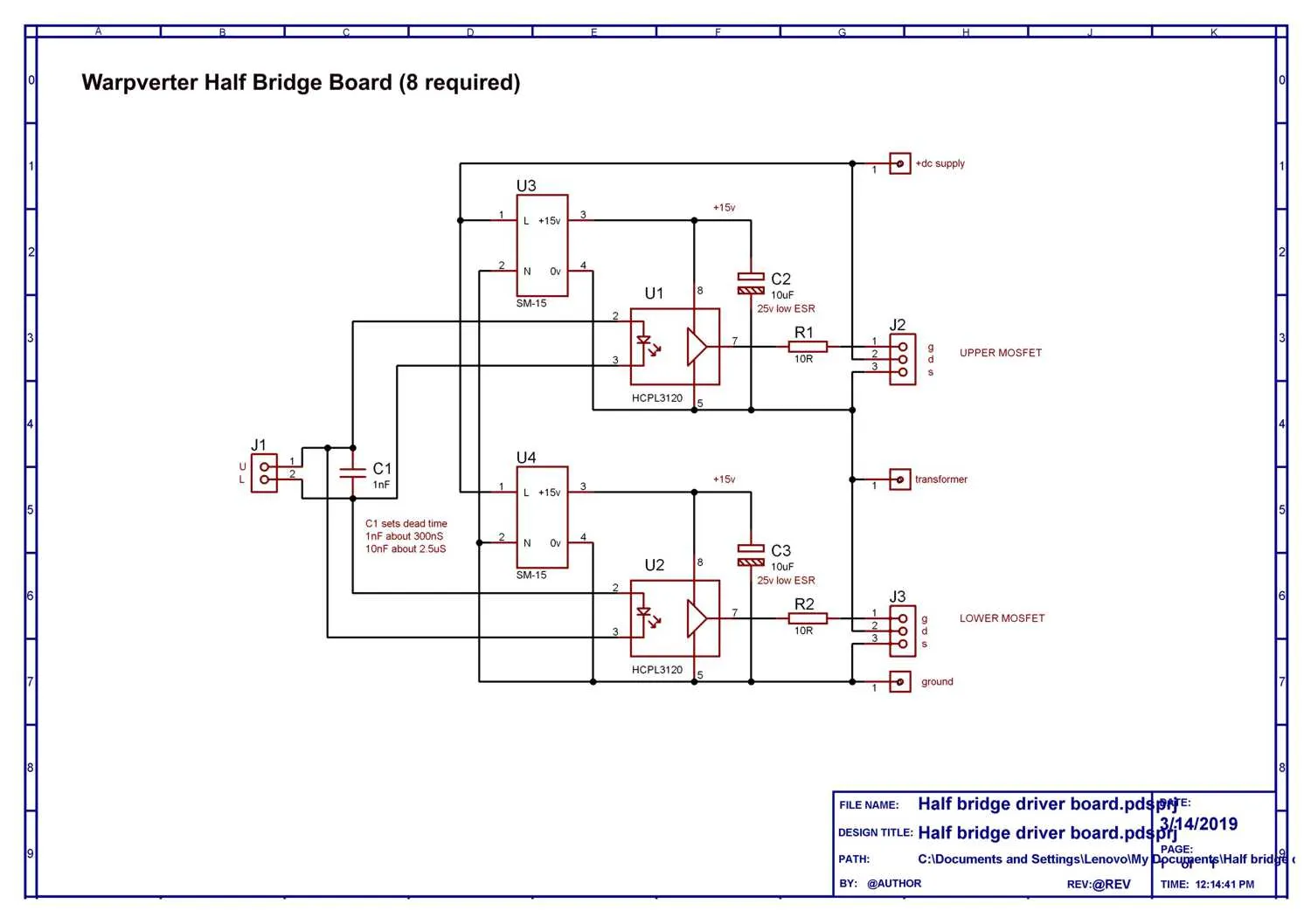
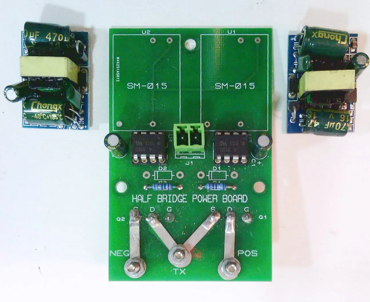
The half bridge driver boards each drive one upper and one lower IGBT on one side of each bridge.
Opto isolators are used, but the opto isolator LEDs are connected in inverse parallel, so it’s impossible for both opto isolators to be on together.
This feature reliably prevents any shoot through problem, where upper and lower IGBT might conduct simultaneously. By adding some capacitance across the opto LEDs, that generates reliable and symmetrical dead time.
All of these features combine to make for a very robust switching bridge that is extremely immune from noise, or corrupted data that may occur during power up or power down, or brownout. Its the secret to designing very robust inverters that do not randomly blow up !
Data comes from the control board over a balanced low impedance twisted pair, that is opto isolated at the far end. This provides extremely high noise immunity and the twisted pairs can be made quite long without any worries about picking up noise. That can be rather important at very high power levels.
One data bit controls one side of the bridge. Logic 0 is lower IGBT on, Logic 1 is upper IGBT on. Always one or the other is on, except during dead time. There are four possible logic drive states to each bridge 00, 01, 10, and 11. All are safe in the respect that corrupted data might put a momentary kink in the sine wave, but it cannot blow anything up.
So basically the whole of the four power switching stages are very well protected from noise or being driven with scrambled or corrupt data. This goes a very long way to designing a very reliable bullet proof inverter.
How the Voltage Regulation Works
The transformers are wound with primaries to suit the lowest incoming dc voltage.
At the lowest design voltage, the transformers are switched to produce the full 81 step voltage range and nominal ac output voltage.
Because the transformer ratios are fixed, increasing the dc voltage would produce a corresponding increase in ac output voltage.
My own Warpverter works between 90v and 180v incoming dc voltage. Yours might be any 2:1 dc voltage range.
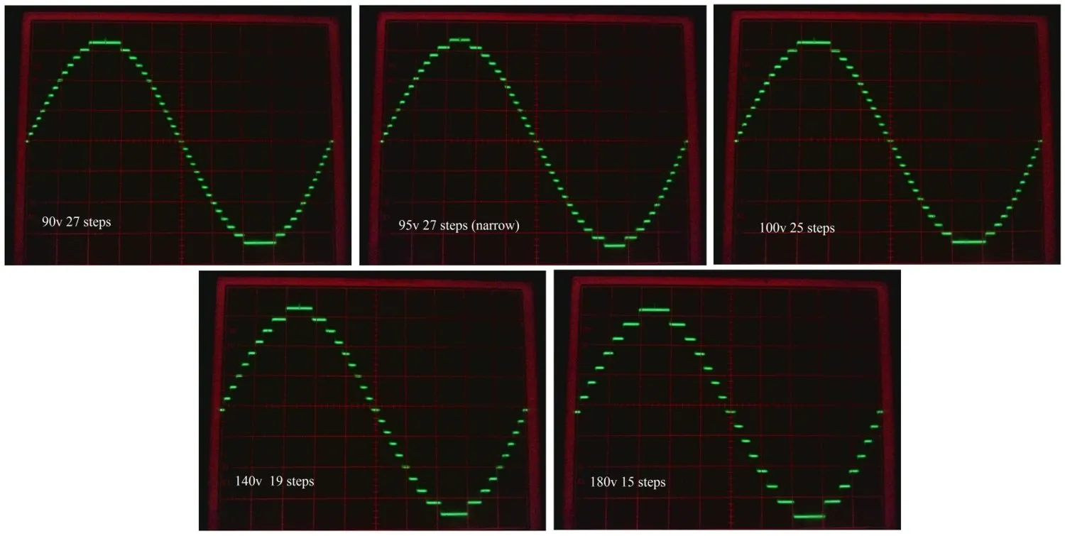
The waveforms shown below are with only three inverters running which produces 27 steps. With fewer steps its much easier to see the changes that occur.
The fourth inverter produces such a smooth sine wave its very difficult to see anything happening.
At minimum dc input voltage of 90v you can see the full 27 steps.
If the input voltage is increased to 95v, notice the top step right at the peak has become slightly narrower. In fact all of the steps are made slightly narrower, but its most noticeable right at the peak.
This overall change in the waveform corrects for the 5v dc increase, producing the same nominal rms ac output voltage.
If we keep slowly increasing the incoming dc voltage, eventually the top step becomes narrower and narrower, finally disappearing, and we have fewer steps peak to peak. This provides very fine output voltage control, and we can have a regulated output voltage over a very wide 2:1 change in dc input voltage.
The change in waveshape is produced by jumping between lookup tables in ROM.
The jump always occurs right at a zero crossing, so large output voltage corrections can be made without causing any discontinuity in the sine wave. There are 256 different lookup tables that cover the 2:1 dc input voltage range.
What determines which lookup table to use is a measurement of the incoming dc voltage. That is measured 25 times each second, and the ac output voltage is fully corrected every second mains cycle right at the zero crossing.
This system does not require any voltage feedback from the output of the inverter.
Its very fast acting compared to feedback, and it can never become unstable in the way feedback sometimes can.
The only disadvantage is that due to slight voltage droop with increasing load in the transformers, and voltage drop in the IGBTs, the ac output voltage does fall slightly with increasing load. In my own inverter its about a ten volt drop at 5Kw of load, compared to zero load.
The grid does that anyway, and it's never been a problem here.
That can be corrected by measuring the DC input current to the inverter and using that to modify which lookup table is selected beyond what the incoming voltage measurement dictates.
I have tested the idea and it works as expected, but have not bothered to build another control board to incorporate it into my own inverter. Other Warpverter builders are using the current measuring modification and are very pleased with it.
This voltage regulation all works backwards when back charging a Warpverter from a grid tie inverter. It still regulates the ac voltage, preventing it from rising when the grid tie inverter is back feeding.
Here are some waveforms showing the effect of different dc input voltages on the ac output with only three inverters running.
The oscilloscope is set for 100v per division.
Ac output voltage is held pretty constant even though the vertical height of each step increases in proportion with the increase in dc input voltage.
Regulated Steps - 90V Input 27 Steps - 180V Input 15 Steps
No Voltage Feedback Used ...
Feed Forward Instead!
One other very unusual feature of the Warpverter is that there is no voltage feedback from the secondary windings required.
The output voltage is regulated using voltage and (optionally) current feed forward instead of feedback.
I have never seen another inverter do that !!!
But this is interesting. It responds much faster to step load changes than feedback ever could.
And it can be tweaked so that the ac output voltage can decrease, stay the same, or increase under increasing load.
It's possible to over compensate for having a very long wiring run between the inverter and load, so that the voltage at the load is well regulated in spite of a large and varying voltage drop in the wiring.
Most inverters use voltage feedback to maintain a constant output voltage with changes of dc input voltage and load.
The main problem with that is its slow to correct.
The correction must be introduced slowly, or it can over correct and become unstable. Sudden large step changes in load (up or down) can cause annoying sags and surges in voltage resulting in light flicker.
The inverter output voltage will eventually settle, and then remain fairly constant.
Feed forward works in an entirely different manner.
The dc input voltage is measured, and the inverter can then very quickly adjust the waveforms driving the output transformers to compensate for any change in dc input voltage. The result is that the reaction time of the inverter to sudden dramatic load change can be made much faster acting.
It can compensate pretty much perfectly for input voltage variation over a very wide 2:1 dc input voltage range.
The down side is that although the transformer primary waveforms are well corrected, the transformer secondary voltages do fall slightly with increasing inverter load.
Voltage droop in my own 5Kw Warpverter is about ten volts (at 240v) from zero load to the full 5Kw rated output. That should be pretty typical, all mainly due to unavoidable voltage drop under load in the transformers.
The grid supply here varies more than ten volts anyway from day to day, and hour by hour, and none of my household appliances seem to mind. So I don't think its necessary to have a precise inverter set output voltage.
What is much more important is to have very fast voltage corrections for sudden step load change, and feed forward correction provides that.
Its especially good at reducing light flicker during the starting of large motors.
Its much easier and faster and more accurate to measure a dc voltage than an ac voltage, which is a constantly changing sine wave at 50/60Hz anyway.
The incoming dc is measured in a dual slope integrating a/d converter (to average out impulse noise) on the dc, and the measured voltage used to address one of 256 different lookup tables in ROM.
These lookup tables cover a 2:1 input voltage range, and allow for a very fine adjustment of inverter output voltage. Large very sudden jumps in voltage correction are possible, and always occur right at a zero crossing, so there are never any waveform discontinuities created from large applied corrections.
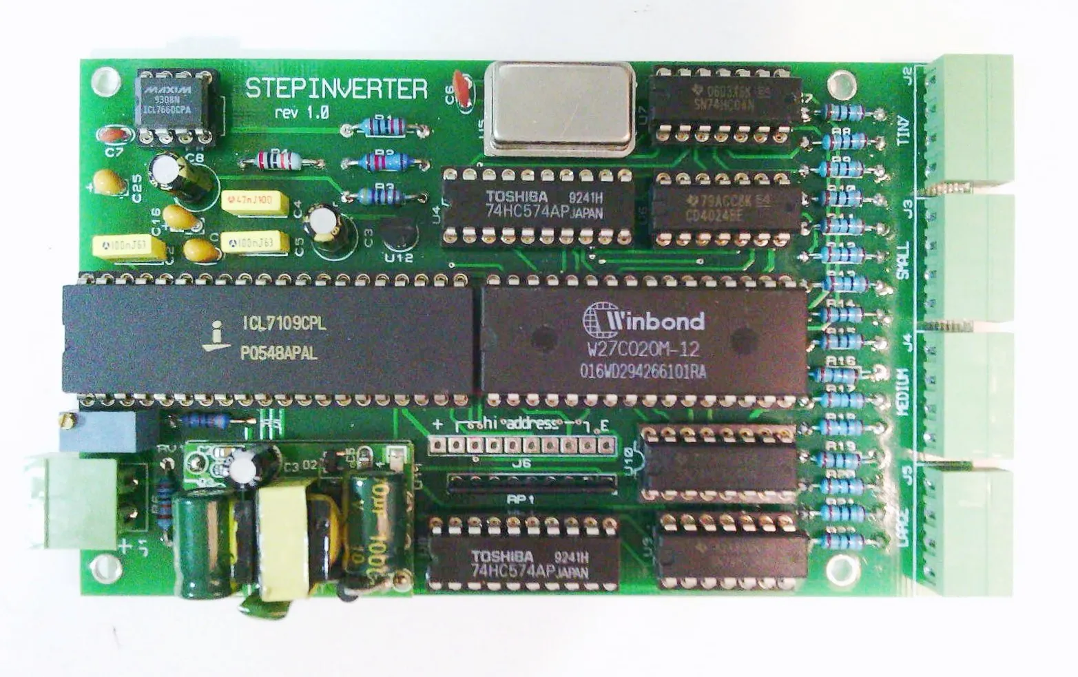
This can all be achieved with some simple robust and reliable hardware. The lookup tables contain direct simple gate drive data to the four power switching bridges, there is no software or data manipulation involved.
Some Random Photos
To see more detail right click and "Open image in new tab"
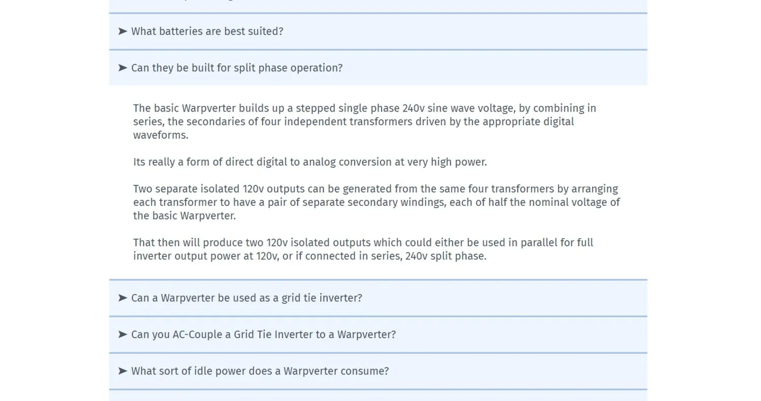
How Split Phase works on a Warpverter
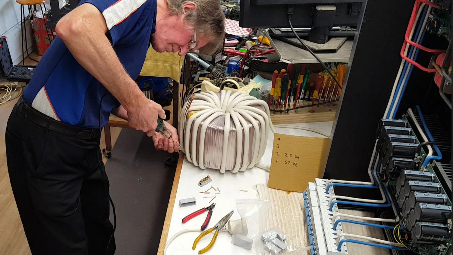
Stripping the enamel off the ends of the individual copper wires using a DF-8 electric wire stripper ... available from Amazon or aliexpress
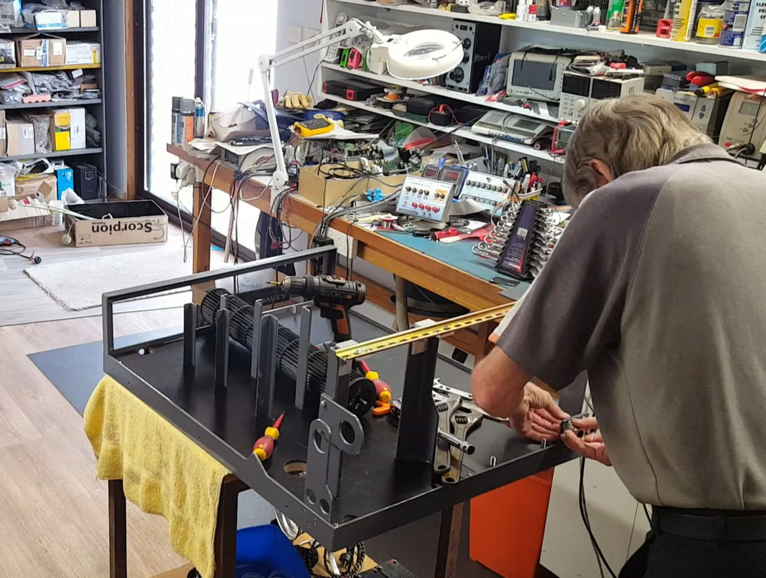
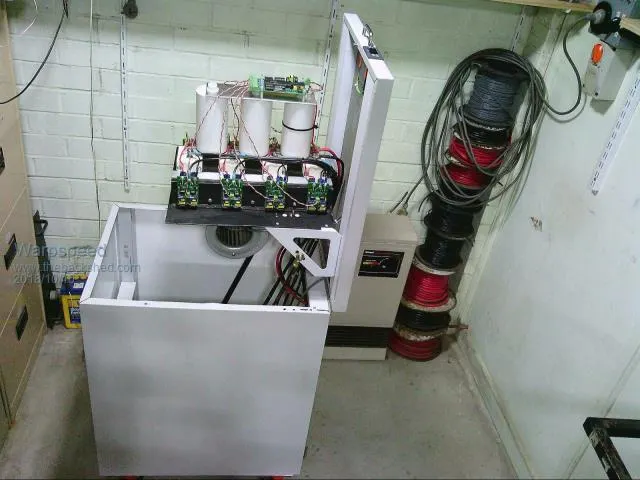
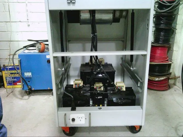
Starting the final assembly
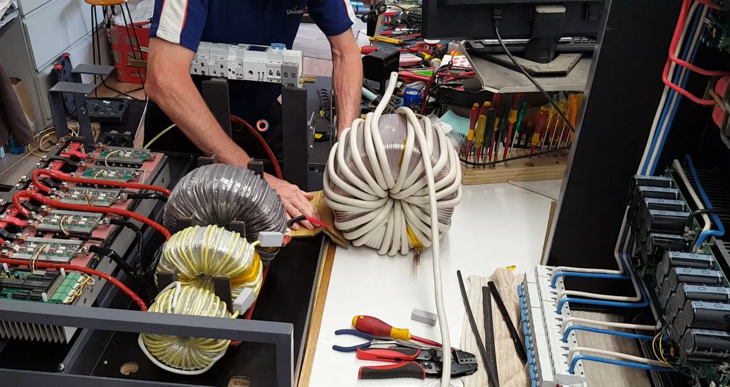
Bit heavy to lift at 57kg, so just rolled into place

Lor
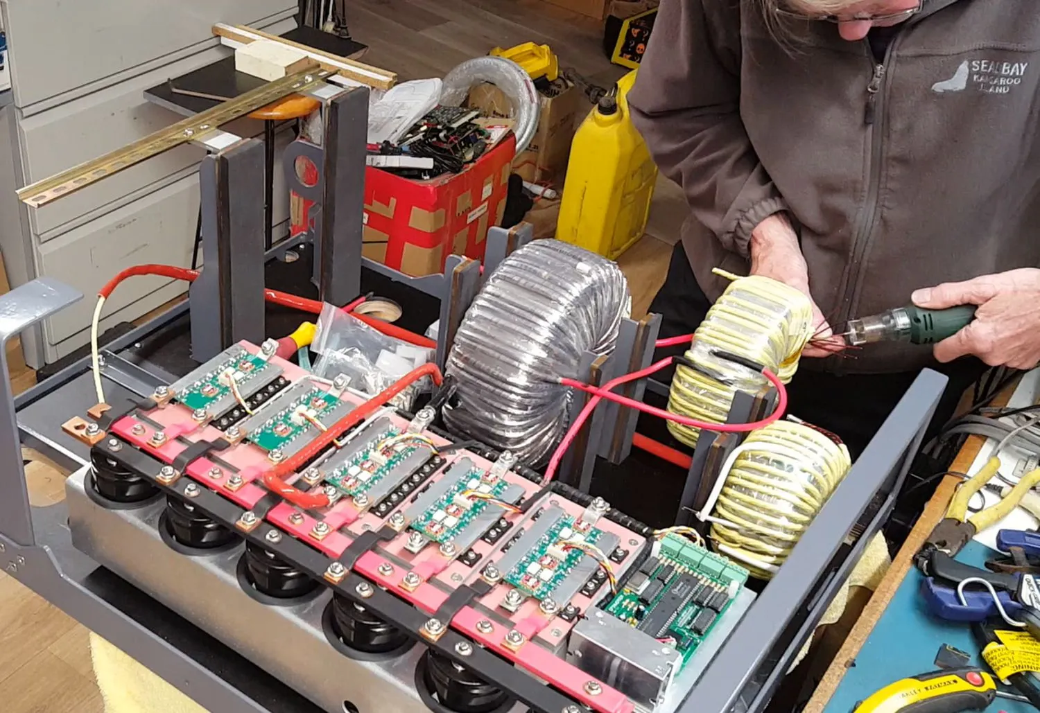
Stripping the wire enamel off the "Small" toroid winding ends
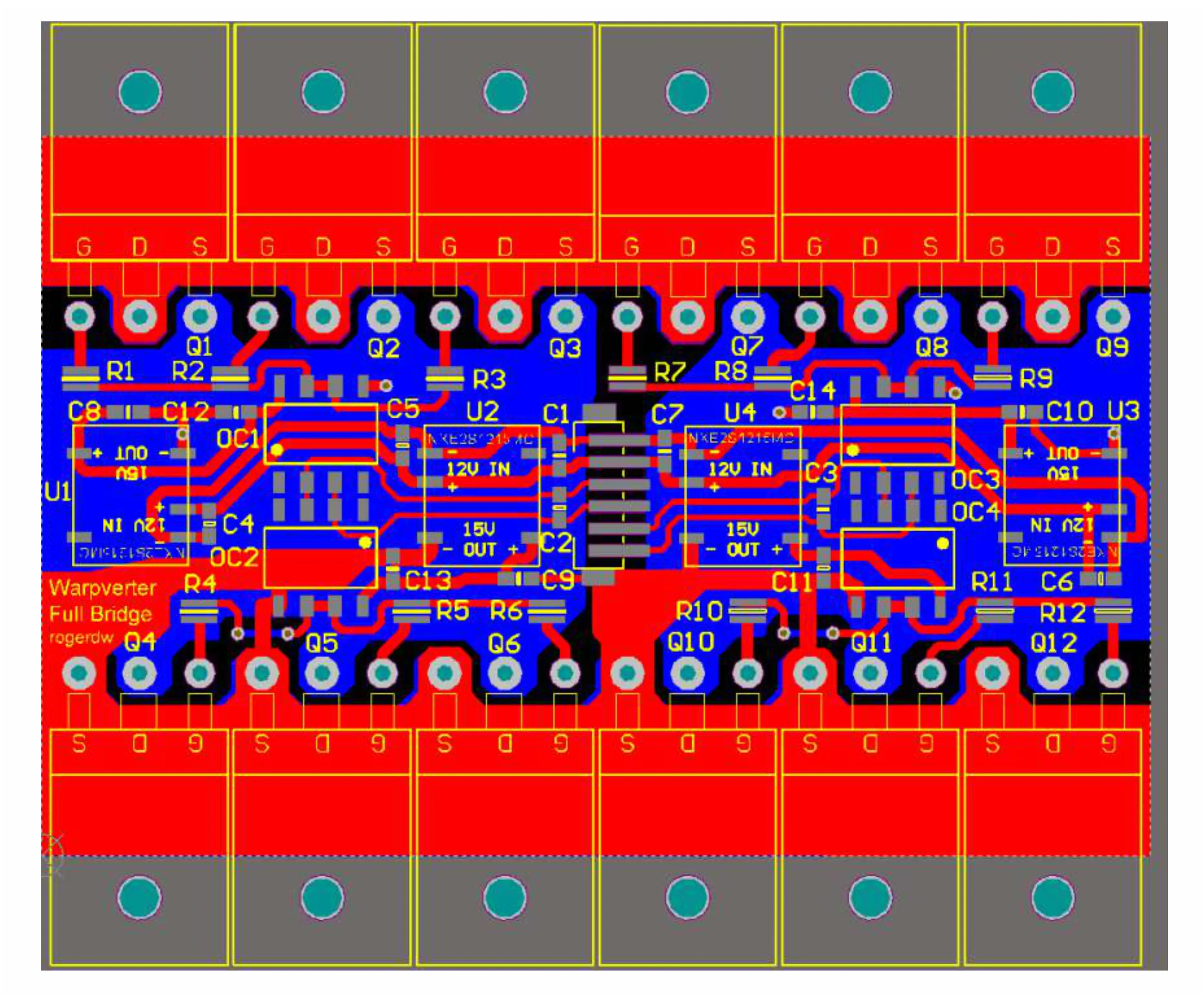
Warpverter Full Bridge board layout
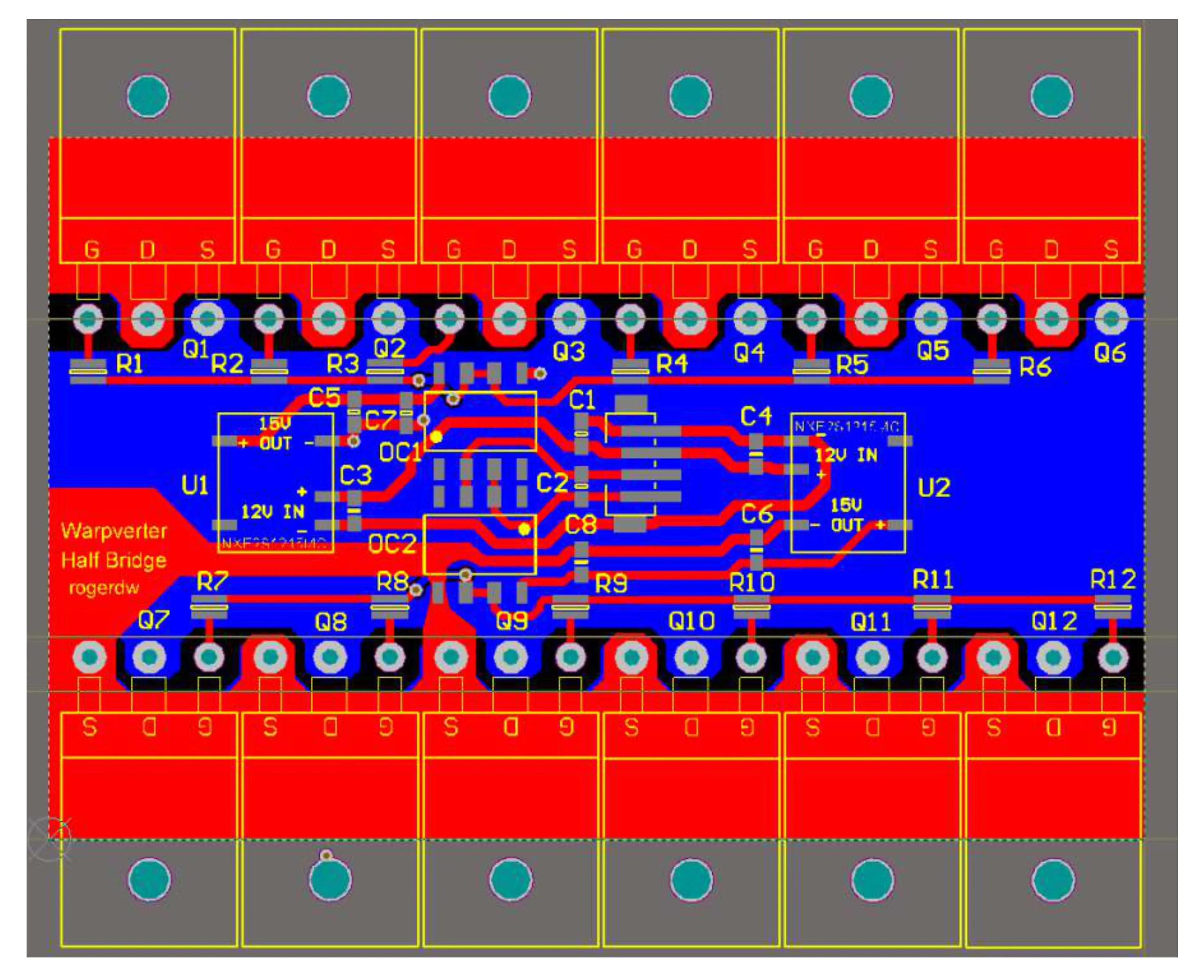
Warpverter Half Bridge board layout
Lorem ipsum dolor sit amet, consectetur adipiscing elit. Quorum altera prosunt, nocent altera.
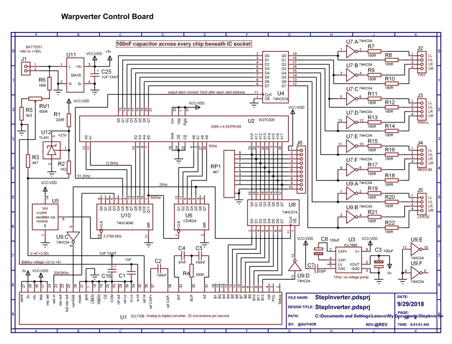
Click Circuits to Open High Resolution Versions
Contact: Visit this thread on diysolarforum and message Warpspeed or rogerdw

© 2024 Warpverter.com - All Rights Reserved. Terms of Service: Privacy Policy:
